C2C/C2W Bonding
Application
- 3DIC, power module packaging, flip welding, etc
- Chip to Wafer hybrid bonding (Cu/PI, Cu/SiO2 hybrid bonding)
- Fine-Pitch bump bonding, solder/copper bump bonding
- Development and mass production of MEMS, optoelectronics and hybrid bonding
Technical advantage
- High precision alignment: ≤±2µm(optional: ≤±1µm, ≤±0.5µm)
- The core module is autonomous and controllable
- Can be customized according to customer needs
- A full range of low temperature bonding solutions are available
- A variety of material activation methods: formic acid activation, plasma activation, low stress low temperature bonding
C2C Bonding
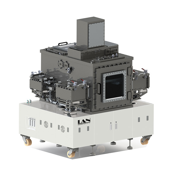
MAFB series C2C
-
Item Parameter Pressure range/controlled pressure stability 0~2000N/3000N:±2N Alignment accuracy ±50nm Post-bonding accuracy ≤±2µm;≤±1µm;≤±500nm Pressure head temperature control range/pressure head temperature control stability RT~300℃/±1℃ Indenter heating rate(RT-250℃) 5min Sample size Top:1*1~50*50mm; Below:2*2~300*300mm Cooling Method Air Atmosphere in Bonding chamber Vacuum、Formic acid、Inert atmosphere, etc -
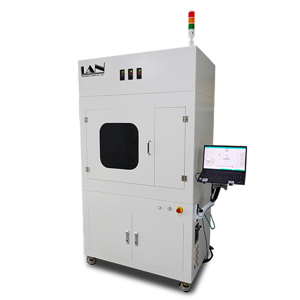
SAFP series small lot C2W
-
Item Parameter Pressure range/controlled pressure stability 1~50N:±0.5N
51~2000N:±2NAlignment accuracy ±50nm Post-bonding accuracy ≤±2µm;≤±1µm;≤±500nm Activation Method Formic acid catalytic activation, etc
Ion activation module (optional) -
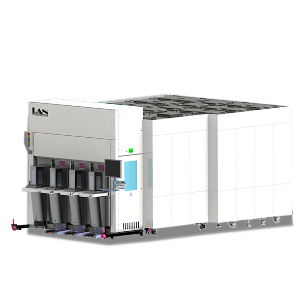
FDWB series Full auto C2W
-
Item Parameter Range of pressure 0~300N Post-bonding accuracy ±200nm/500nm@3σ Alignment accuracy ±50nm Chip size 1*1—32*32mm Wafer size φ300mm TF Station 2 FOUP Station 2 UPH 400 Capacity of Application Cu-SiO2 hybrid bonding;SiO2-SiO2Low temperature bonding Equipment units Activation, cleaning, lifting, alignment, bonding, inspection -