Wafer bonding Systems
Application
- Composite substrate manufacturing SOI,POI,etc
- wafer level hybrid bonding for CIS and memory chip manufacturing
- MEMS, Microfluidic devices, LED and other manufacturing
Technical advantage
- A variety of bonding technologies: ultra-high vacuum room temperature bonding, hydrophilic bonding, hot pressing bonding
- The wafer can be bonded at room temperature or low temperature to reduce the impact of thermal stress
- A variety of alignment methods, can achieve sub-micron level of high precision alignment
- Comprehensive solutions
- Can be customized according to customer needs
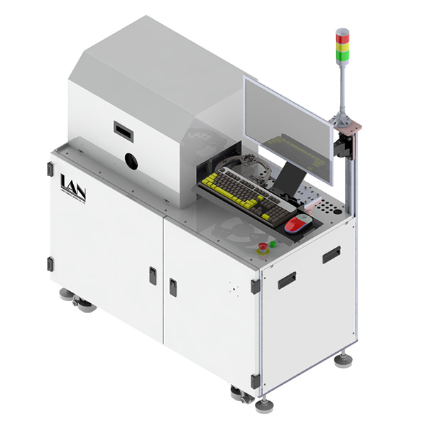
Room temperature wafer bonding Equipment
ED series R&D model
-
Item Technical Parameters Wafer size ≤12 inch,and fragments Applicable Si、LT、LN、Sapphire、InP、SiC、GaAs、 GaN、Diamond, metal, glass, organic materials, etc UPH 1 pair/h Loading mode Manual Maximum pressure of the pressurized system 80kN Surface treatment method In-situ surface activation&sputter deposition Bond strength ≥1.5J/m2@room temperature(Si-Si/glass-glass bond) -
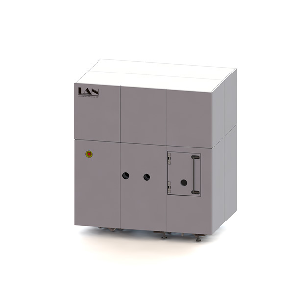
SD series Standard production model
-
Item Technical Parameters Wafer size 4-8 inch Applicable Si、LT、LN、Sapphire、InP、SiC、GaAs、 GaN、Diamond, metal, glass, organic materials, etc UPH ≥6pair/h Loading mode cassette(Manual) Maximum pressure of the pressurized system 100kN Alignment method and accuracy Edge alignment accuracy≤±50µm
mark alignment≤±2µmBond strength ≥1 .5J/m2@room temperature(Si-Si bond) -
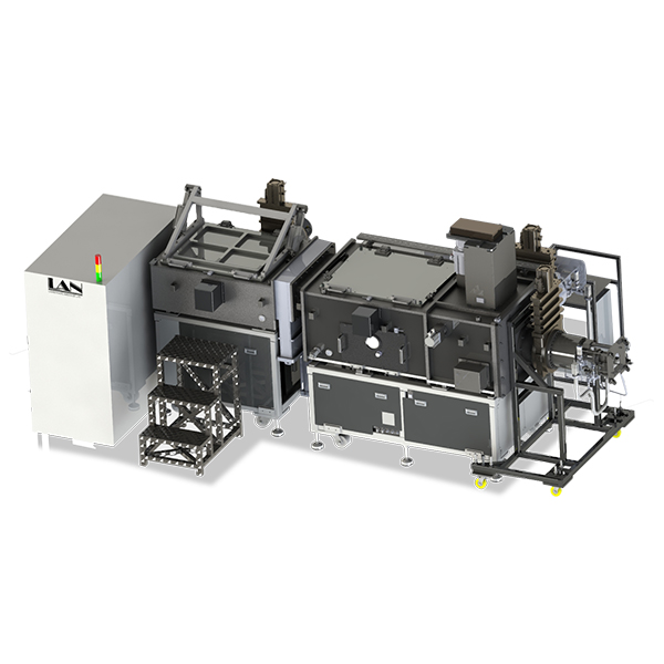
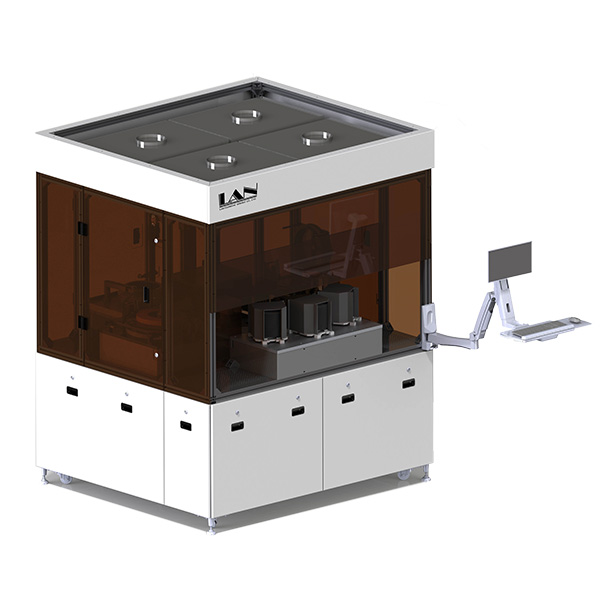
CSAB series -Cluster production model
-
Item Technical Parameters Wafer size 6-8 inch Applicable Si、LT、LN、sapphire、InP、SiC、GaAs、GaN, metal, glass, organic materials, etc UPH ≥10pair/h Loading mode cassette(Manual) Maximum pressure of the pressurized system 100kN Alignment method and accuracy Edge alignment accuracy≤±50µm
Mark alignment (option)≤±2µmBond strength ≥1.5J/m2(Si-Si direct bonding) -
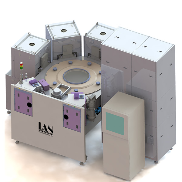
Hydrophilic wafer bonding Equipment
Production Model
-
Item Technical Parameters Wafer size 6-12 inch Applicable SOI、POI、Hybrid Bonding UPH ≥14pair/hr Load mode cassette(Manual) Alignment accuracy ≤±50µm/±0.2µm/±50nm(option) Bond strength ≥2.0J/㎡(Si-Si bond after anneal)) DI water clean Standard Liquid cleaning Standard -
Hot press anode bonding Equipment
ACWB
-
Item Parameter Wafer size D:50mm-300mm Applicable Glass,Sapphire,Metal ,etc. Maximum temperature 550℃ Pressing force (Max.) 100kN Rate of warming 30℃/min Temperature heterogeneity ≤±1% Anode voltage ≤1kV Anode current ≤100mA -